Emerging Technology and Materials Cleanrooms

Description
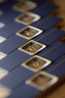
Microfabrication Equipment Our Microfabrication capability provides flexible opportunities for development of front-end processing and multifarious research in semiconductor device physics and technology.
Equipment and capability within the ETM Group includes:
Lithography
•EMS 5000 Spin Coater •SLEE Co. Mask Aligner •Karl Suss MJB-3 Aligner •Minimum feature size: 1.5 µm •Alignment accuracy +/- 1 µm (front side align) •Hotplate and oven baking •Lift-off process (image reversal) •Spin coating of photoresists and polyimides Wet Processing
•Two class 100 vertical laminar flow work stations with extraction. Both stations are equipped with •Ultrasonic baths •The Veolia Water Systems Ltd. PURELAB Ultra source of ultrapure water •Chemically resistant hot plates •Nitrogen jets Deposition of metals and dielectrics
•Oxford Instruments FlexAL 200mm Atomic Layer Deposition tool •Oxford Instruments Plasmalab System 400 DC & RF magnetron sputter tool; •equipped with 4 inch RF and two 8 inch DC magnetrons for metals and dielectrics sputtering •Two individual Kurt J. Lesker PVD 75 vacuum deposition systems. •Each sputter deposition system contains two targets for magnetron sputtering. •One machine is fitted with two DC power sources and the second machine has one DC and one RF/DC power source. •BOC-Edwards Auto thermal evaporator fitted with four evaporation boats •BOC-Edwards Auto e-beam evaporator fitted with four hearth crucible deposition of wide range of materials including refractory metals. Thermal Processing
•JIPELEC rapid thermal processing furnace specified for SiC post-implantation annealing; •annealing at temperatures up to 2000°C in argon and nitrogen •Two custom made oxidation furnaces; •oxidation in nitric oxide, dry and wet oxygen; •JetFirst 200 bench top RTP processor; •RTP at temperatures up to 1200°C in high vacuum, nitrogen, oxygen, ammonia and forming gas; Plasma Processing
•TEGAL Co. PLASMOD microwave asher •Plasma-Therm 790 series RIE machine. •RIE of silicon, silicon carbide, silicon dioxide, poly-silicon, polyimide, etc. using SF6, CHF3, O2, Ar gases and mixtures •Resist stripping and descum Packaging
•TCB-21e Dage Precima Bonder Process Control Equipment
•Carl Zeiss Interference Microscope •Leitz Wetzlar Optical Microscope •Tencor P-1 Long Scan Profiler •KSV Instruments CAM-100 Contact Angle Meter •Filmetrics F40 Thin Film Thickness Measurement System •Probe station with Tektronix 577 curve tracer
Characterisation Lab The ETM Group has a climate controlled electrical and material characterisation facilities that provides the opportunity to perform an extensive array of tests on semiconductor devices and structures. Test capabilities include:
•DC and RF 200mm probe stations for varied C-V and I-V analysis to 67GHz •low and high frequency noise measurement •specialist facilities in electrical measurement for hostile environments •Atomic force microscopy •Raman
ManufacturerVarious
ModelVarious
Contact
Academic Contact
| Professor Nick Wright | |
| nick.wright@ncl.ac.uk |
Technical Contact
| Tracey Nicholls | |
| tracey.nicholls@ncl.ac.uk |